How to Specify an FR4 Custom PCB Board for High-Voltage and High-Heat Designs
A high-voltage, high-heat board should be specified from the electrical and thermal stress outward, not from a default FR4 datasheet inward. A laminate described simply as “FR4” does not establish whether the finished assembly will retain insulation margin, survive repeated thermal cycling, or dissipate heat from power components without localized damage. The specification needs to connect operating voltage, waveform, contamination exposure, conductor geometry, copper distribution, component temperatures, and fabrication capability.
Begin with the actual voltage seen by each insulating path. Nominal bus voltage is only one input. Switching overshoot, ringing, fault states, surge events, and the voltage difference between adjacent nets can create a much higher local stress. A layout carrying a moderate DC voltage may still require generous spacing when a fast-switching node sits beside a low-voltage control trace, mounting hardware, a shield, or an accessible metal feature.
Define the Electrical Insulation Problem Before Selecting Material
For an FR4 custom PCB board, dielectric strength is useful as a material property, but it is not a substitute for clearance and creepage design. Dielectric strength describes breakdown through the laminate under a defined test condition. Clearance is the shortest distance through air between conductive features. Creepage follows the board surface, where dust, condensation, residue, and aging can lower insulation resistance. Each failure route behaves differently.
A thick board does not automatically solve a surface insulation problem. Increasing overall thickness can improve the distance through the substrate between layers, yet it does little for closely spaced pads or traces on the same outer layer. Conversely, a wide surface gap does not ensure sufficient insulation between copper planes separated by a thin prepreg layer. The fabrication drawing should therefore identify the voltage difference associated with critical conductor pairs and distinguish outer-layer spacing from inner-layer dielectric requirements.
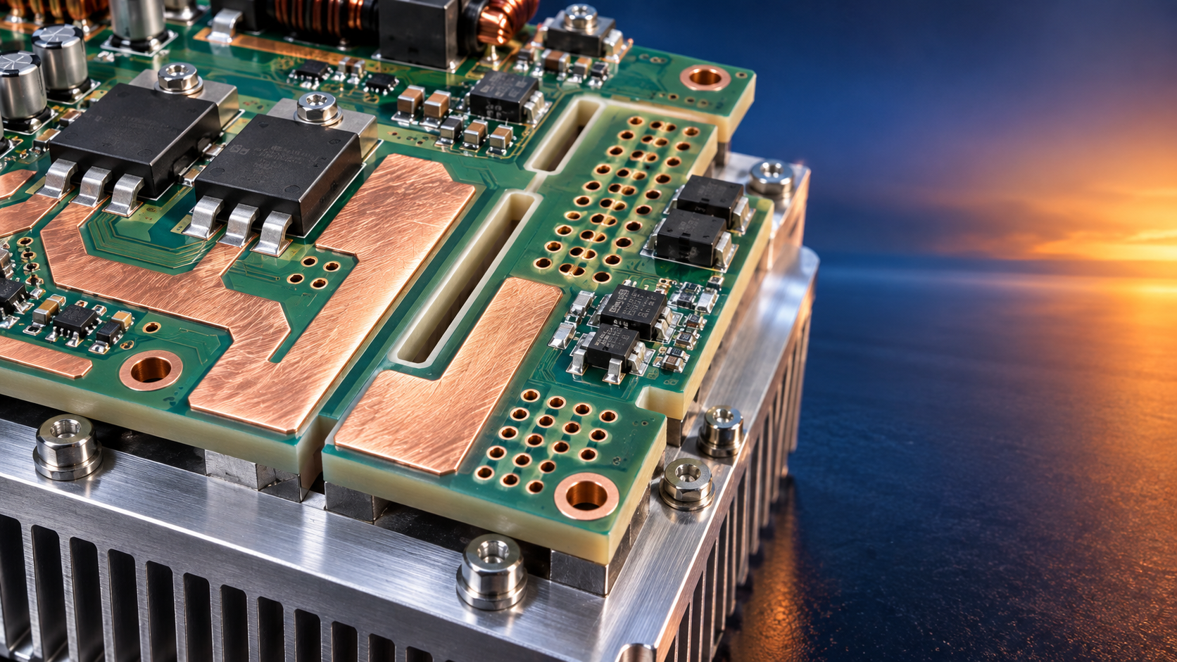
Slots and routed isolation barriers can increase creepage where board area is constrained. Their benefit depends on the real geometry after fabrication and assembly. Copper pullback from the routed edge, plating requirements, solder mask coverage, component body overhang, adhesive residue, and nearby hardware all need review. A slot that appears to separate two nets in a layout can lose part of its value if a metal fastener, heatsink, or connector shell bridges the effective path in the completed product.
Choose a Thermal Grade by the Full Temperature Profile
Standard FR4 is a family of glass-reinforced epoxy laminates rather than one uniform construction. For high-temperature duty, the important questions are the laminate’s glass transition behavior, its expansion through and above that transition region, its decomposition resistance, resin system, and the temperature limits imposed by the finished assembly. These values should be taken from the selected material family and construction, not copied from a generic FR4 assumption.
Glass transition temperature alone is often overinterpreted. A board can operate below that value and still be stressed by copper imbalance, mechanical clamping, repeated heat-up and cool-down, or plated-through-hole expansion. Once a resin system softens, its dimensional behavior changes substantially; repeated excursions near that region can increase strain on vias, pads, and solder joints. A design with short but frequent high-temperature cycles can be harder on interconnects than one with a higher but stable ambient temperature.
Specify the expected temperature at the board hot spot, not merely the enclosure ambient. Power semiconductor leads, transformer pins, shunts, rectifier areas, and isolated gate-drive regions frequently create local temperatures well above a sensor placed elsewhere in the enclosure. Include the assembly process profile too. Lead-free reflow, selective soldering, hand rework, and repeated repair exposure can impose different thermal loads. A laminate selected for operating temperature but not for assembly exposure leaves an avoidable reliability gap.
Thermal conductivity in ordinary FR4 is limited, especially through the thickness of the board. Thick copper spreads heat laterally, but it does not turn the laminate into an efficient vertical heat path. When a component must transfer heat to an opposite-side copper area, use a deliberate thermal route: an adequately sized copper land, an array of thermal vias where electrical isolation permits, controlled via fill or plugging when solder wicking is a concern, and an interface to a chassis or heatsink designed around real contact pressure. If electrical isolation to the heatsink is required, evaluate that interface as part of the thermal model rather than assuming the PCB alone will carry the load.
Translate Current and Heat Into Copper Requirements
Copper weight should be specified layer by layer. Saying “heavy copper board” does not indicate which layers carry current, whether the stated weight is base copper or finished copper after plating, or how narrow features are allowed to become after etching. Outer layers gain copper during plating; inner layers do not. The same nominal copper weight can therefore produce different finished thicknesses and different etch behavior across the stack-up.
Trace width calculations must include conductor temperature rise, ambient conditions, copper thickness, permitted voltage drop, and whether heat can spread into adjacent copper. A short high-current trace connected to a large copper region behaves differently from an isolated track of the same width. Neck-downs at component pads, fuse footprints, vias, connector pins, and current-sense features deserve separate analysis because they may become the hottest point even when the main route is broad.
Heavy external copper also changes manufacturability. Fine-pitch components, narrow isolation gaps, small annular rings, and dense solder-mask dams become less forgiving as copper thickness rises. Etching creates sidewall geometry rather than perfectly vertical edges, so a finished narrow gap may differ from the value assumed in a nominal CAD rule. State the smallest conductor width and spacing at the required finished copper thickness, then confirm that the fabricator can hold those values across the panel and selected material construction.
Where layers have very different copper coverage, specify whether copper balancing or thieving patterns are acceptable. Uneven copper distribution can contribute to bow and twist, uneven plating, and local thermal distortion. Adding nonfunctional copper can help manufacturing consistency, yet it must not compromise creepage paths, create unwanted capacitive coupling, or form a heat-spreading route that moves heat into temperature-sensitive circuitry.
Make the Stack-Up a Controlled Deliverable
For voltage and heat-sensitive work, a layer count and total thickness are insufficient. Request a proposed stack-up showing each core and prepreg construction, copper weight before and after processing where applicable, finished dielectric thicknesses, and the resin system. The layer pair carrying the highest voltage differential deserves explicit callout. Do not leave the dielectric separation between those layers to a standard construction selected after the design is released.
Prepreg behavior deserves particular care when wide copper planes sit beside sparse routing. During lamination, resin flows to fill spaces and bond layers. Copper pattern density influences the remaining dielectric thickness after pressing. A nominal prepreg designation does not guarantee the same cured thickness everywhere. Where insulation margin is tight, work from a fabricator-confirmed finished stack-up and avoid relying on a calculated thickness that excludes resin flow effects.
Controlled impedance may coexist with high-voltage requirements, especially in converter control, communications, sensing, or gate-drive sections. These constraints can conflict: impedance targets often favor a closely coupled reference plane, while insulation needs favor greater dielectric separation. Separate zones or different layer assignments may be preferable to forcing one stack-up rule across the entire board. A high-energy switching region should not dictate an unnecessarily thin dielectric beneath a low-voltage signal layer merely to simplify routing.
Vias, Holes, and Board Edges Need Their Own Review
Plated-through holes are mechanical and electrical transition points. In a high-heat design, via barrel reliability depends on hole size, finished board thickness, plating quality, thermal cycling, and the local copper pattern. Very small holes in a thick board increase aspect ratio and make uniform plating harder. Large copper pads connected to hot components can increase local stress, particularly where repeated cycling occurs. State minimum finished hole sizes, whether vias may be tented, filled, plugged, or left open, and whether any via carries current or is part of a thermal path.
Board edges and mounting holes are frequently missed during insulation review. A conductive chassis, screw head, washer, standoff, shield, or heatsink may become the nearest conductive object rather than the adjacent PCB trace. Define copper-to-edge pullback, copper-to-mounting-hole clearance, and any non-plated isolation holes. If the board is panelized with V-scoring, consider whether the remaining web, breakout geometry, and depanelization process could damage copper near a high-voltage boundary.
Mask should be treated as a protective process layer, not the only planned insulation barrier. Solder mask thickness, coverage quality, and long-term surface condition vary with geometry and processing. Mask openings around pads, exposed test points, and rework areas create locations where the effective insulation path differs from the artwork view. When a protective coating is part of the design intent, document its coverage boundaries, cure expectations, and exclusions around connectors, switches, thermal interfaces, or high-voltage gaps.
Release Data That Prevents Ambiguity at Fabrication
The fabrication package should communicate performance intent without trying to dictate every factory process setting. Include the approved material family or acceptable alternatives, finished thickness tolerance, copper weights by layer, finished stack-up, minimum trace and gap requirements, drill table, routing and slot details, surface finish constraints, and controlled-impedance notes where applicable. Clearly mark net classes or drawing regions associated with elevated voltage. A generic note asking for “high-voltage clearance” cannot be inspected consistently because it does not identify which features are subject to that requirement.
Request fabrication feedback before production when a specified feature approaches a process limit. The most useful questions are concrete: whether the requested finished dielectric can be achieved after lamination, whether the copper and spacing combination remains producible, whether routing tolerances preserve the isolation slot, and whether thermal vias need a different treatment to support assembly. The response should be tied to the actual stack-up, not a broad statement that the design is “manufacturable.”
Inspection criteria should reflect likely failure mechanisms. Visual inspection can reveal mask voids, copper burrs, insufficient pullback near routed edges, and contamination around isolation features. Electrical testing verifies continuity and unintended shorts, but it does not by itself prove long-term creepage performance under humidity and heat. Where the application requires additional dielectric or environmental verification, define the test method, test points, acceptance condition, and whether the test applies to bare boards or completed assemblies.
Resolve Conflicting Requirements Early
The difficult cases are usually not caused by one inadequate parameter. A compact board may demand wide high-current paths, wide high-voltage separation, dense control routing, and direct heat transfer to a metal enclosure in the same area. Increasing copper can improve current capacity while reducing routing space. Enlarging a thermal pad can spread heat while bringing a hot node closer to other conductors. A thicker dielectric can improve isolation but alter impedance and make thermal transfer less effective.
Record these tradeoffs at the level of specific interfaces: switching node to control trace, power plane to chassis, thermal pad to opposite-side copper, and mounting hole to high-voltage area. That approach produces a specification that can be reviewed against real geometry and fabrication output. The final board definition should state the required electrical separations, material behavior, thermal paths, and tolerances together, because each one changes the practical meaning of the others.
Get weekly intelligence in your inbox.
No noise. No sponsored content. Pure intelligence.
 Oct 08, 2026How Digital Health Improves Diagnostic Accuracy and Workflow in Clinical LabsHow Digital Health Improves Diagnostic Accuracy and Workflow in Clinical Labs
 Oct 07, 2026Selecting Voice Picking Systems for German Warehouses: Integration, Languages and ROISelecting Voice Picking Systems for German Warehouses: Integration, Languages and ROI
 Oct 06, 2026How to Choose Last Mile Dispatch Software for On-Time Delivery at ScaleHow to Choose Last Mile Dispatch Software for On-Time Delivery at Scale
 Oct 05, 2026Vietnam’s Consumer Electronics Market: Demand Shifts and Sourcing OpportunitiesVietnam’s Consumer Electronics Market: Demand Shifts and Sourcing Opportunities
 Oct 04, 2026Digital Health Investment Priorities for Providers: Improving Access, Outcomes, and EfficiencyDigital Health Investment Priorities for Providers: Improving Access, Outcomes, and Efficiency
 Oct 03, 2026How to Specify an FR4 Custom PCB Board for High-Voltage and High-Heat DesignsHow to Specify an FR4 Custom PCB Board for High-Voltage and High-Heat Designs
 Oct 02, 2026ERP Software Market Intelligence: Adoption, Pricing, and Vendor Signals to WatchERP Software Market Intelligence: Adoption, Pricing, and Vendor Signals to Watch
 Oct 01, 2026How to Select Calibrated Temperature Data Loggers for GMP Cold Storage MonitoringHow to Select Calibrated Temperature Data Loggers for GMP Cold Storage Monitoring
 Sep 30, 2026Custom Molded Rubber Pricing: What Drives Unit Cost and Tooling Fees?Custom Molded Rubber Pricing: What Drives Unit Cost and Tooling Fees?
 Sep 29, 2026How to Evaluate Energy Management Software Vendors for Multi-Site OperationsHow to Evaluate Energy Management Software Vendors for Multi-Site Operations
 Sep 28, 2026How to Select a DIN Rail Smart Meter for Multi-Circuit Energy MonitoringHow to Select a DIN Rail Smart Meter for Multi-Circuit Energy Monitoring
 Sep 27, 2026TWS Earbuds in Vietnam: Demand Drivers, Price Tiers, and Retail Channel OpportunitiesTWS Earbuds in Vietnam: Demand Drivers, Price Tiers, and Retail Channel Opportunities
 Sep 26, 2026How UAE Clinics Can Qualify a Smart Glucometer Supplier for Accuracy and ComplianceHow UAE Clinics Can Qualify a Smart Glucometer Supplier for Accuracy and Compliance
 Sep 25, 2026Buying Aesthetic Lasers in the USA: FDA Status, Wavelengths, and Service SupportBuying Aesthetic Lasers in the USA: FDA Status, Wavelengths, and Service Support
 Sep 24, 2026Laser Cutting Brass Sheet: How to Prevent Burrs and Heat Marks on Thin PartsLaser Cutting Brass Sheet: How to Prevent Burrs and Heat Marks on Thin Parts
 Sep 23, 2026How to Choose Lightweight ANC Headphones for Comfortable All-Day TravelHow to Choose Lightweight ANC Headphones for Comfortable All-Day Travel
 Sep 22, 2026IPX5 TWS Bluetooth Earbuds: What Protection Do They Offer for Workouts?IPX5 TWS Bluetooth Earbuds: What Protection Do They Offer for Workouts?
 Sep 21, 2026What to Look for in a Grid Integration Company for Utility-Scale Solar ProjectsWhat to Look for in a Grid Integration Company for Utility-Scale Solar Projects
 Sep 20, 2026Microgrid Controller Pricing: What Drives Cost in Commercial Energy Projects?Microgrid Controller Pricing: What Drives Cost in Commercial Energy Projects?
 Sep 19, 2026How to Choose a GaN Charger for Laptops Without Compromising Power or PortabilityHow to Choose a GaN Charger for Laptops Without Compromising Power or Portability
 Sep 18, 2026Floating Solar Farm Costs: CAPEX, OPEX, and the Site Factors That Shape ROIFloating Solar Farm Costs: CAPEX, OPEX, and the Site Factors That Shape ROI
 Sep 17, 2026Drone Delivery Solutions for Last-Mile Routes: Site, Payload, and Range PlanningDrone Delivery Solutions for Last-Mile Routes: Site, Payload, and Range Planning
 Sep 16, 2026When Low-Volume Electronics Manufacturing Makes More Sense Than Mass ProductionWhen Low-Volume Electronics Manufacturing Makes More Sense Than Mass Production
 Sep 15, 2026Wholesale WiFi Smart Switches: What Buyers Should Verify Before OrderingWholesale WiFi Smart Switches: What Buyers Should Verify Before Ordering
 Sep 14, 2026How to Select IoT Sensors for Reliable Monitoring in Harsh Industrial EnvironmentsHow to Select IoT Sensors for Reliable Monitoring in Harsh Industrial Environments
 Sep 13, 2026How Procurement Teams Can Improve Supplier Reliability With Supply Chain VisibilityHow Procurement Teams Can Improve Supplier Reliability With Supply Chain Visibility
 Sep 12, 2026Smart Manufacturing Trends 2026: What Leaders Should Prioritize for ROISmart Manufacturing Trends 2026: What Leaders Should Prioritize for ROI